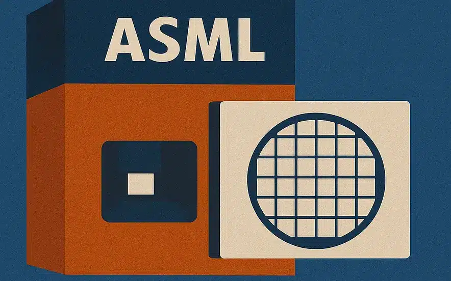
ASML EUV machines are at the center of the next chipmaking revolution. In the heart of the Netherlands, behind highly secured doors in ASML’s cleanroom, sits a technological marvel that’s reshaping our digital future. For the first time ever, we’ve been granted exclusive access to film inside the facility housing the world’s most advanced chipmaking machine the $400 million High NA EUV lithography system.
The Silicon Kingmaker: Why ASML’s Technology Rules the Chip World
The global AI revolution has one critical dependency that few outside the semiconductor industry fully appreciate: extreme ultraviolet lithography (EUV). Without these remarkable machines, the advanced chips powering everything from your smartphone to cutting-edge AI systems simply couldn’t exist.
ASML, headquartered in Veldhoven, Netherlands, holds a complete monopoly on this technology. Every advanced chipmaker – from Nvidia and Apple to Taiwan Semiconductor, Samsung, and Intel – depends entirely on ASML’s EUV systems to manufacture their most sophisticated chips.
The Next Generation: High NA EUV Explained
High NA (Numerical Aperture) represents the next evolutionary leap in chipmaking technology. These machines, standing taller than a double-decker bus, are the culmination of decades of research and billions in investment.
“It still does blow my mind,” says Ayssia Haddou, who leads the team testing and qualifying High NA machines. “I think even if you learn more about it, it blows your mind even more.”
What makes High NA special? These systems use the same extreme ultraviolet light source as previous EUV machines but with a critical difference – they capture light at steeper angles through larger lens openings, allowing them to print increasingly minuscule designs in fewer steps.
Inside the $400 Million Marvel: How High NA EUV Works
The process begins with molten tin being shot out at an astonishing 50,000 droplets per second. These tiny droplets are vaporized with powerful CO₂ lasers, creating explosions that emit photons of extreme ultraviolet light at a wavelength of just 13.5 nanometers – roughly the width of five DNA strands side by side.
“We use four [CO₂ lasers] to shoot at one of these tiny tin droplets to generate a plasma, which is hotter than the sun,” explains Jos Benschop, an ASML veteran who helped spearhead the company’s first foray into EUV technology.
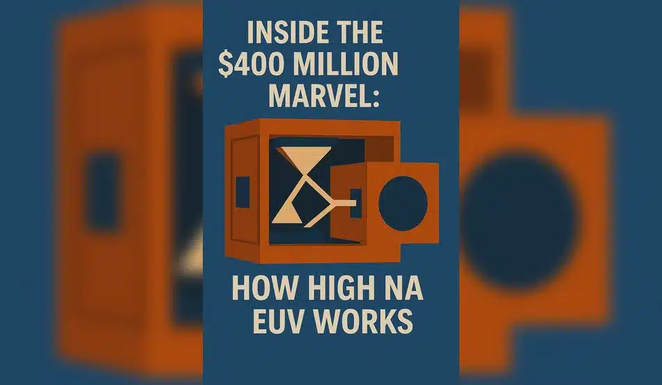
This light is so small it gets absorbed by almost everything, requiring the entire system to operate in a vacuum. The EUV light bounces off specialized mirrors made by German optics company Zeiss – the flattest man-made surfaces in the world – before being projected onto silicon wafers coated with photoresist chemicals.
The precision required is mind-boggling. Taiwan Semiconductor Manufacturing Company (TSMC) describes it as equivalent to “shining a laser from the moon to hit a coin on Earth.”
The Global Impact: Why High NA Matters for AI and Beyond
While ASML sold only 44 EUV machines in 2024 (compared to 374 cheaper DUV machines), these advanced systems accounted for 38% of the company’s system sales revenue due to their $220 million price tag. The newer High NA machines command an even higher price at around $400 million each.
Why would companies invest such astronomical sums? The answer lies in Moore’s Law – the observation that the number of transistors on a microchip doubles approximately every two years while costs are halved.
“The cost of the chips the tool is going to create is going down,” explains Christophe Fouquet, ASML’s CEO. “Moore’s Law says that we need to continue to drive costs down. This allows you to go to the next node and then the next node, and then again the next node. If this was to stop, then everyone gets stuck.”
🔬 Discover Careers Behind ASML EUV Machines Powering AI Chips
Fascinated by the future of chipmaking and AI hardware?
Step inside the world of ASML EUV machines — the groundbreaking technology enabling the next generation of high-performance AI chips in 2025.
WhatJobs helps you explore cutting-edge tech roles in semiconductor engineering, photolithography, and AI-driven manufacturing.
👉 Browse high-tech job openings now — and shape the future of innovation.The AI Connection: Powering the Next Computing Revolution
High NA technology is arriving at a critical moment in computing history – the explosive growth of artificial intelligence. These advanced chips are essential for training and running sophisticated AI models.
However, this technological advancement comes with significant energy demands. “If we don’t improve the power efficiency of our AI chips over time, the training of the models could consume the entire worldwide energy, and that could happen around 2035,” warns Fouquet.
ASML has been working diligently to address this concern, reducing “the energy needed per wafer exposure by more than 60%” since EUV’s introduction in 2018.
The Global Semiconductor Landscape: Geopolitics and High NA
The semiconductor industry has become a focal point of international politics, with the U.S. implementing export controls that prevent ASML from selling its EUV machines to China. This ban, which began during the first Trump administration, aims to limit China’s access to the most advanced chipmaking technology.
Despite these restrictions, China has been stockpiling ASML’s less advanced machines. “We had a huge backlog in China because we got orders in 2022 at the peak of the market,” notes Fouquet. “End of 24, last quarter, the part of China in our business went down to 30%.”
The American Expansion
While Asia has traditionally made up over 80% of ASML’s business, the U.S. share (around 17% in 2024) is growing rapidly as companies like Intel build new chip fabrication plants in Ohio and Arizona, and TSMC expands its Arizona operations.
ASML’s workforce has grown from 32,000 employees in 2022 to 44,000 today, with 8,500 based in the United States across 18 offices. The company is also bringing its first U.S. training facility to Arizona, capable of training 1,200 people annually on EUV technology.
Learn more about semiconductor manufacturing trends in 2025
The Future: Hyper NA and Beyond
ASML isn’t resting on its laurels. The company is already developing its next-generation technology, dubbed “Hyper NA,” which will enable even smaller features on chips.
When asked about the rumored $700 million price tag for these future machines, Fouquet responds, “Oh, it’s way too early to mention the number, but typically price goes up. So no, I don’t think it’s going to be that high.”
Despite current market uncertainties, including potential impacts from tariffs, ASML expects customers will need Hyper NA technology between 2032 and 2035.
The Global Chip Race: Can Anyone Challenge ASML?
ASML’s monopoly on EUV technology raises an important question: could another company – or country – develop competing technology?
“I feel like it’s a real long shot that China could enter this space,” notes one industry expert. “But right now, China’s really figuring out ways to take things like seven nanometer, the most advanced nodes that can be done without EUV, and figuring out ways to scale them.”
This technological leadership comes with responsibility. “While this is a monopoly right here and today, in the era of AI, there will be new vehicles for building semiconductors,” cautions another observer. “If I’m ASML, if I’m from any other company in this space, I’m being careful to make sure that I’m protecting my position, not just in the near term, but in the long term as well.”
The Logistics Challenge: Shipping $400 Million Machines
Moving these enormous machines presents a logistical challenge of epic proportions. Each High NA machine is made up of four subsystems manufactured in Connecticut, Germany, the Netherlands, and California.
“It takes about seven Boeing 747s to ship this whole thing, and it’s about 25 to 30 trucks,” explains an ASML representative. The modules are assembled and tested at ASML’s headquarters before being disassembled again for shipping to customer facilities.
What This Means for the Future of Technology
ASML’s High NA EUV lithography machines represent more than just advanced manufacturing equipment – they are the cornerstone of our technological future. From smartphones and autonomous vehicles to artificial intelligence and quantum computing, these machines enable the increasingly powerful chips that drive innovation across every sector.
As we look toward a future where computing demands continue to grow exponentially, ASML’s technology will remain at the heart of this revolution, printing the invisible patterns that power our digital world.
Hiring? Post Jobs in Advanced Technology
Looking for skilled professionals in semiconductor technology and advanced manufacturing? Post jobs for free with WhatJobs.
Need Career Advice?
Interested in pursuing a career in the cutting-edge field of semiconductor manufacturing? Explore opportunities and get expert guidance on the skills needed for this high-tech industry.
Get Semiconductor Career Advice
FAQ: ASML High NA EUV Lithography Technology 2024
What is ASML’s High NA EUV lithography technology?
ASML’s High NA EUV lithography technology is the world’s most advanced chipmaking system, using extreme ultraviolet light with a higher numerical aperture to print incredibly small features on silicon wafers for advanced semiconductor manufacturing.
Why is ASML’s High NA EUV technology important for AI development?
ASML’s High NA EUV technology is crucial for AI development because it enables the production of more powerful, energy-efficient chips needed for training and running sophisticated AI models, without which advanced AI systems would be impossible to create.
How much does an ASML High NA EUV machine cost?
An ASML High NA EUV lithography machine costs approximately $400 million, making it one of the most expensive pieces of manufacturing equipment in the world, with the company shipping only about five systems in 2024.
Which companies are using ASML’s High NA EUV technology?
Companies using ASML’s High NA EUV technology include Intel, TSMC (Taiwan Semiconductor Manufacturing Company), and Samsung, with Intel being the first to implement the technology in its Oregon chip fabrication plant.